| | CB Radio Frequency Synthesis We felt duty-bound to give some basic theory, here, but the explanations will be kept as short as possible. Hopefully this small section will help the beginners to acquire some idea of what Frequency Synthesis is all about. Those of you who know it all, already, can skip this bit. For more information read Lou Franklin's "CB PLL DATA BOOK". If that is still not enough (clever clogs) there are plenty of textbooks about!
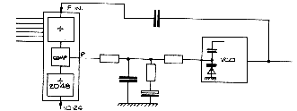
1. The VCO is an oscillator circuit whose frequency is determined by the capacitance of a varactor diode. The capacitance of this diode is controlled by the reverse-bias voltage applied to it. (Since the diode is reverse-biased, virtually no current flows).
2. The PLL chip is an I.C. with three main sections:-
a) A digital frequency divider (DFD).
b) A programmable DFD.
c) A phase detector (PD) which effectively compares the output frequencies of the two DFDs and produces an output voltage according to the difference between the frequencies.
Operation: A crystal oscillator feeds 10.24MHz into the first DFD which divides by (typically) 2048 to produce a 5kHz reference signal within the PLL chip. The VCO oscillates at an arbitrary centre frequency which is sampled and fed to the second DFD. The PD provides a voltage to raise or lower the VCO frequency until the divided result equals 5kHz. The circuit is then said to be "in lock".
Notes: The PD output is not pure D.C. so a low pass filter network is used to remove switching transients. The filter capacitor must be large enough to provide adequate smoothing without making the circuit response time too long. Larger value capacitors have a series resistor to prevent "ringing".

Fig 1.
The programmable DFD enables the divide ratio to be selected.
General purpose PLL chips such as PLL02A, MC145106P, MC145151P, MB8719 have no internal memory. The divide ratios are determined exactly by the channel selector codes plus the codes on the remaining inputs.
Those PLL chips designed specifically for operation in just one country have an internal memory which contains only those divide ratios which produce the permitted frequencies. The divide ratios are accessed by the binary codes from the channel selector switch. There is no specific mathematical relationship between the channel selector codes and the divide ratios in the memory.
Eproms
An Eprom is a memory I.C. and contains a large number of memory cells, each of which can be filled with eight binary digits i.e. 1s or 0s.
A memory cell can be selected by putting the appropriate access code of 1s and 0s on the input pins. The contents of that cell will then be displayed as 1s and 0s on the output pins of the I.C.
For instance, if we put the code 11100000 into the cell whose access code is 11100000 then effectively the output duplicates the input. If we encode all memory cells with their own access codes then connect the Eprom between the channel switch and the DFD input of the PLL chip, there will be no effect on the operation of the synthesiser circuit.
This seems a little pointless, however there are only 40 possible channel selector codes but several thousand memory cells. If we encode only those 40 cells accessed directly by the channel selector (which will give the standard frequencies), we still have several thousand cells left in which to put other codes for different frequencies.
The channel selector switch will have from 6 to 8 outputs which may be connected to the access pins of the Eprom. However, the Eprom has ten or more access pins; consequently by using a band switch to put codes on the spare access pins we can select different banks of memory cells which can be programmed to give various frequency bands. For more information on the use of Eproms see the "CB EPROM DATA BOOK".
With dedicated ICs, such as the LC7137, reprogramming is not possible as the codes are stored in internal memory. With ICs like the MC145106P, however, we can use divide ratios between approximately 10 and 320. Such ICs lend themselves readily to external reprogramming. Note, however, that they will not work at frequencies much greater than 3 MHz. The MC145151 is an exception and will work at more than 30 MHz.
To sum up, then: with these versatile ICs the manufacturers saved money by designing the channel switch, itself, to present the divide ratios (in binary form) directly to the IC programming pins. Sometimes, as in the case of the later Cobra 148 GTL, a couple of binary adder ICs (MC14008B) are interposed between the channel switch and the synthesiser IC. Extra codes can thus be added to the switch codes to alter the programming information. It is generally easier for us to use an Eprom and encode it with the codes we need for the required channels.
Changing Crystals
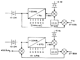
Virtually all the CB synthesisers you will see use a 10.24 MHz crystal to produce a 5 kHz or a 10 kHz reference within the IC (or sometimes a choice of either). This reference frequency actually determines the channel spacing. If, therefore, you try to produce extra channels by substituting, say, a 10 MHz crystal then you may get your 40 channels, but the channel spacing will be 9.766 kHz, not 10 kHz. Also, if the IC uses different codes for TX and RX you will receive on a channel far removed from that on which you transmit. Even this difficulty can be overcome by using different crystals for TX and RX (although the channel spacing will still be awry) but a further problem remains: 10.695 - 10.24 = 455 kHz which is the 2nd I.F. 10.695 - 10.0 = 695 kHz which is not; so unless you use a separate 10.24 MHz oscillator to feed the second mixer you will not receive very much!
On the following pages we go into this problem in somewhat greater detail.
Example: Expanding the LC7137 (Used in early UK radios)
Fig.2 shows the normal 10.24 MHz reference crystal connections to the LC7137. Changing the reference crystal is a quick way to add extra channels. It is also a quick way to end up transmitting on one channel and receiving on another if you don't understand what you are doing!
We carried out some computer calculations using various "surplus" crystals which could be obtained at a very reasonable price. The table following shows the result of switching in different reference crystals for receive and transmit. Note how the RX and TX frequencies gradually drift apart in the columns marked "D Hz". An error of up to about 500 Hz is tolerable but communication becomes distorted and range is considerably reduced if the discrepancy is significantly higher than this.
Since the Intermediate Frequency relies upon the result of 10.695-10.240=0.455 it is essential to add a separate 10.24 MHz oscillator.
 Fig.2 Fig.2
The table shows how difficult it is to produce useable channels with crystals other than the correct reference frequency of 10.240 MHz. It is also evident that the further the new crystals are removed from 10.240, the smaller the number of useable channels produced, because the inter-channel spacing becomes much less than 10kHz and the variation in channel spacing between TX and RX increases.
First crystal pair Second crystal pair Ch. 10.1137 10.1625 10.09235 10.00000
rx MHz tx MHz D Hz rx MHz tx MHz D Hz
40 27.7767 27.7782 1478 27.5846 27.5864 1765
39 27.7668 27.7682 1430 27.5749 27.5766 1675
38 27.7569 27.7583 1383 27.5651 27.5667 1585
37 27.7471 27.7484 1335 27.5554 27.5568 1495
36 27.7371 27.7385 1287 27.5456 27.5470 1405
35 27.7273 27.7285 1240 27.5358 27.5371 1314
34 27.7174 27.7186 1192 27.5261 27.5273 1224
33 27.7075 27.7087 1144 27.5163 27.5174 1134
32 27.6977 27.6988 1097 27.5065 27.5076 1044
31 27.6878 27.6888 1049 27.4968 27.4977 954
30 27.6779 27.6789 1001 27.4870 27.4879 863
29 27.6680 27.6690 954 27.4772 27.4780 773
28 27.6582 27.6591 906 27.4675 27.4681 683
27 27.6483 27.6491 858 27.4577 27.4582 593
26 27.6384 27.6392 811 27.4479 27.4484 503
25 27.6285 27.6293 763 27.4382 27.4386 412
24 27.6187 27.6194 715 27.4283 27.4287 322
23 27.6088 27.6094 668 27.4186 27.4189 232
22 27.5989 27.5995 620 27.4089 27.4090 142
21 27.5890 27.5896 572 27.3991 27.3992 52
20 27.5792 27.5798 524 27.3893 27.3893 -38
19 27.5693 27.5698 477 27.3796 27.3794 -129
18 27.5594 27.5598 429 27.3698 27.3696 -219
17 27.5495 27.5500 382 27.3600 27.3597 -309
16 27.5396 27.5400 334 27.3503 27.3499 -399
15 27.5298 27.5301 286 27.3405 27.3400 -489
14 27.5199 27.5201 239 27.3307 27.3302 -580
13 27.5100 27.5102 191 27.3210 27.3203 -670
12 27.5001 27.5003 144 27.3112 27.3105 -760
11 27.4902 27.4904 96 27.3014 27.3006 -850
10 27.4803 27.4804 48 27.2917 27.2907 -940
9 27.4705 27.4705 0 27.2819 27.2809 -1030
8 27.4606 27.4606 -47 27.2722 27.2710 -1121
7 27.4507 27.4507 -95 27.2624 27.2612 -1211
6 27.4408 27.4407 -142 27.2526 27.2513 -1301
5 27.4310 27.4308 -190 27.2429 27.2415 -1391
4 27.4211 27.4209 -238 27.2331 27.2316 -1481
3 27.4112 27.4110 -285 27.2233 27.2217 -1572
2 27.4014 27.4010 -333 27.2136 27.2119 -1662
1 27.3915 27.3911 -381 27.2038 27.2020 -1752
Note: the "D Hz" column is calculated from the 8 digit frequencies of which only 6 figures are printed in this table. Since the reference frequency is now taken from crystals which no longer divide down exactly to 5 or 10kHz (e.g. 10.240/2048 = 5kHz) the channel spacing is slightly less than 10kHz.
| |


 Fig.2
Fig.2